| ● Wafer Loaders for IC Inspection Microscopes NWL200 Series |
| ● OPTISTATION 3000 |
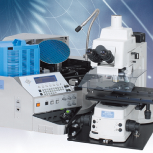
| Wafer Loaders for IC Inspection Microscopes NWL200 Series
|
| Nikon's newest and most sophisticated wafer loader for IC inspection microscopes.
|
| The NWL200 series is the first lineup of wafer loaders for inspection microscopes capable of loading 100 micron thin wafers. Thanks to a new chuck system, the NWL200 series achieves highly reliable loading suitable for inspection of next-generation semiconductors. Improved wafer-sensing functions also help prevent damage to wafers, while wafer edge-chipping detection automatically detects edge-chipping defects.
|
 |
In the semiconductor manufacturing process, wafers are following a trend toward ever greater thinness. Nikon's outstanding proprietary technology makes the NWL200 Series the first lineup of wafer loaders for inspection microscopes capable of loading 100 μm thin wafers. The NWL200 Series achieves highly reliable loading suitable for inspection of next-generation semiconductors.
|
|
| Macro Inspection Functions
|
| In addition to pattern side macro inspections of all areas, macro inspection of the back side periphery and back side center are supported as standard. Macro inspection parameters such as wafer rotation speed and tilt angle can be set automatically or manually. Use the macro setting knobs to preset initial settings and make further adjustments using the joystick. In addition, the new WIL-LED illumination system enables more uniform illumination over a wider area. Various illumination systems are available, from spot lighting to uniform wide area lighting.
|

|
| Non-angled, on-axis images
|
 |
Not only is the elevator surprisingly fast, but the non-contact centering mechanism makes it possible to perform alignment quickly and accurately. The multi-arm system also allows loading and unloading of wafers with complete precision, increasing the overall efficiency of transfer and wafer exchange. This dramatically decreases cycle times, achieving levels of throughput never seen before in any other system.
|
|
| Wafer-Slot Buttons
|
 |
The new wafer-slot buttons on the front panel allow users to select any wafer from its slot with a single button. In addition, the large and prominent LCD panel allows users to set the conditions such as the sampling and inspection patterns, and to check the operating status and the content of errors at a glance. The screens are arranged in a hierarchical structure with one screen for each task, resulting in an intuitive dialog format for smooth progress through the steps. A comprehensive suite of file management functions for carriers, samples and so on is useful for automating inspection.
|
|
| Modified Design Offers Improved Ergonomics
|
 |
To ensure operation in a natural posture, ergonomic efficiency is designed into every aspect of the system. Operation keys and knobs are located within easy reach of the operator, so that operation requires minimum movement of the hand or eye. The wafer carriers are located at the front and 35° to the left of the operator, making it easy to load carriers and to check the wafers inside the carriers visually
|
|
| Improved Wafer-Sensing Functions
|
| Since thin wafers can undergo significant distortion in the carrier, the arm may damage them if the position sensors are not accurate. In the past, it was difficult for sensors to read distortion of the wafers accurately, but with optimized arrangement of the wafer sensor beams, the NWL200 Series can accurately detect the shape of thin wafers in the cassette.
|

|
| OPTISTATION 3000
|
| Built upon Nikon's proven front end process technology, the OPTISTATION 3000 offers high-precision, ultra-fast inspection for 300mm wafers. |
| Its efficient transfer sequence, new robotic arm, FOUP opener, and enhanced macro observation functions all contribute to especially high yield rates ? making the OST-3000 a high throughput wafer inspection powerhouse. In addition, the system provides the highest system reliability in its class, using a safety design that complies with SEMI standards.
|
 |
Simple and speedy manual visual inspection of 300mm wafers. Contributes to dramatic increases in yields as an inline inspection system and analysis tool for R&D defect analysis.
|
|
| Enhanced Macro Observation Functions
|
In addition to macro surface inspection, the system comes standard with perimeter inspection and the center of wafer back sides.
The control of rotation speed and tilt angle during macro inspection can be manually adjusted from the default position using a joysitck.
|

|
| High Transfer Stability |
The OPTISTATION-3000 inherits a system that boasts the high system stability and high-transfer rate, proven in front in front end process, of the review system OPTISTATION series.
The system provides the highest system reliability in its class, using a safety design that complies with SEMI standards.
|
| New System Enables Transfer of Warped Wafers |
A new robotic arm for transferring warped wafers has been developed on proprietary Nikon technology.
Nikon's special robotic arm, wafer contact technology, and support sequence enable the safe and sure transfer of highly warped wafers.
|
| Combined Transfer for 200-300mm Wafers on a Single Unit |
 |
Loading a 200-mm cassette adapter enables the combined transfer of 200-300mm wafers on a single unit.
There is no need for bothersome adjustments when making inch-size changes thanks to the load port's auto recognition of cassettes and the design of two-size shared parts. System uptime is thereby dramatically improved. |
|